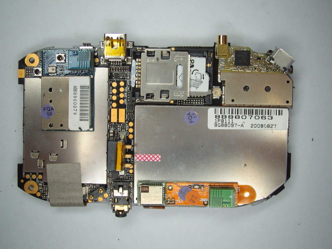
The Internal Debug Board
The case of the
Openmoko
Neo 1973 and
FreeRunner
contains large pockets of
Embedded Air. Here is a little project that puts them to good use:
it integrates the principal functionality of the Openmoko
Debug
Board — USB access to a serial console and to
JTAG — into the Neo itself.
There is also an IDBG variant for the
Ben NanoNote.
Repository:
git clone https://github.com/wpwrak/idbg.git
Design
The Internal Debug Board (IDBG) is designed to provide the following
features:
- Connects directly to USB (Micro-USB, for space reasons)
- IDBG firmware can be updated with DFU
- IDBG gives access to the Neo serial console
- IDBG gives access to JTAG
- IDBG can act as a master on the I2C bus
- IDBG handles the model-specific signals
nGSM_EN (GTA01) and nNOR_WP (GTA02)
- If it is not used, the IDBG is transparent to the rest of the system
Note that not all of this has been implemented and tested so far.
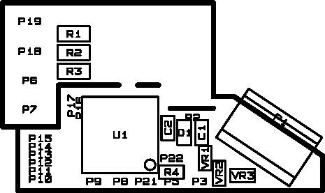
Illustrated build process
The board consists of a
SiLabs
C8051F326
microcontroller (QFN-28, 0.5mm pitch), the micro-USB B connector, and a few
discrete components (mainly 0402). The PCB itself is single-sided with 8mil
traces and 5mil clearance between traces. The circuit is designed for DIY
PCB production using the
toner transfer
method and manual soldering.
KiCad
sources for schematic and layout are in the repository.
Postscript versions of the files can be downloaded by clicking on the
images below.


IDBG comes with a sub-board that gives access
to the signals needed for programming the internal Flash of the
microcontroller. This sub-board is called the "IPL" board, for
Initial
Program Load.
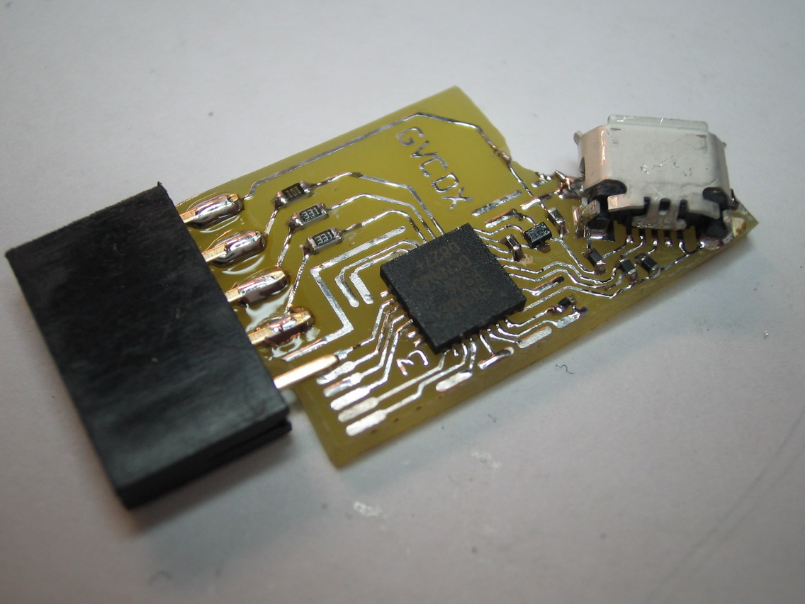
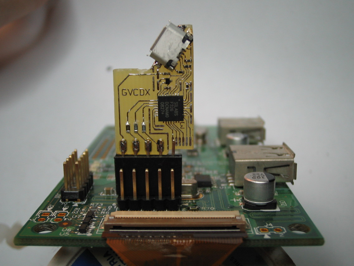
On the left picture we see the IDBG board alone, on the right picture
it is mounted on a Debug Board v3 (v1 and v2 are not suitable but the
board could also be wired directly to the Neo).
In this configuration, power can be supplied
through a GPIO pin and basic communication with the microcontroller
is possible, e.g., to perform a boundary scan.
For Flash programming, USB must be connected to provide additional power.
A simple Flash programmer
called f326 that runs on the Neo is included in the git repository.
Please consult the README for further details.
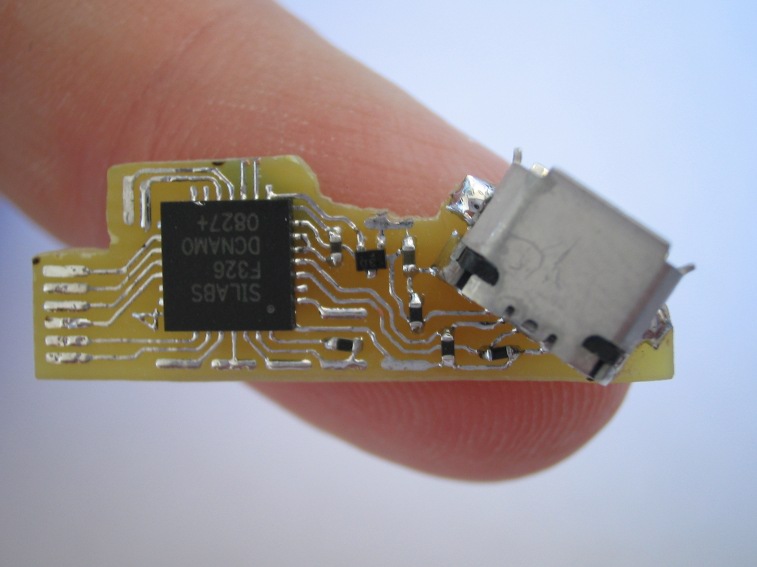
After the initial programming, the IPL sub-board is cut off and the IDBG
board is glued on top of the GPS shield.

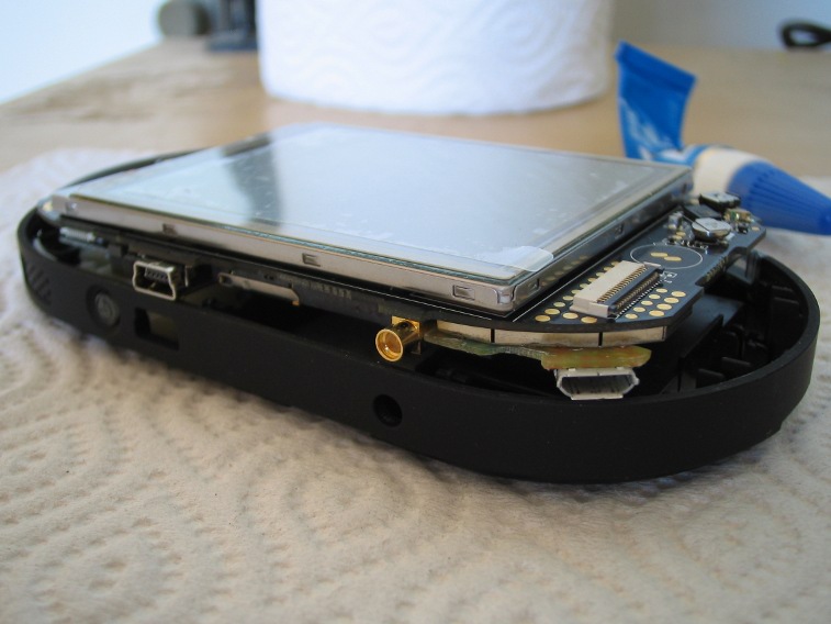
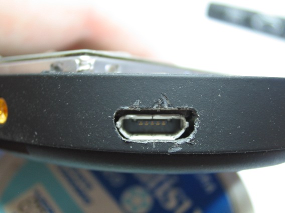
Next, we make a hole for the USB receptacle in the Neo's case. The
picture on the left shows the general lay of the land. Cutting the hole
is a process of trial and error and requires some patience.
It helps to remove only about a millimeter of material at a time and then
to check the position of the connector, as shown in
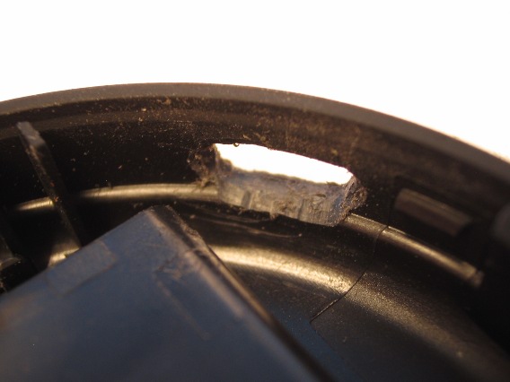
the middle. On the right, we see the final hole from the inside.
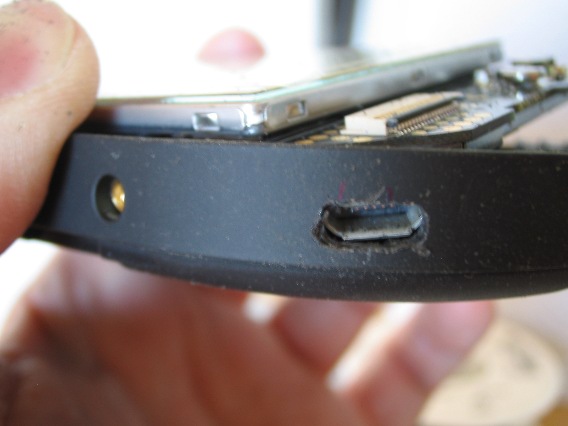
The result should look like my clumsy attempt on the left, but hopefully a bit
more precise and with fewer scratches. The IDBG's PCB may shine through if
the hole is too high. This can be hidden by painting the edge black with a
permanent marker. On the right, we see what the Neo now looks like. It is
important that the entire case closes properly.

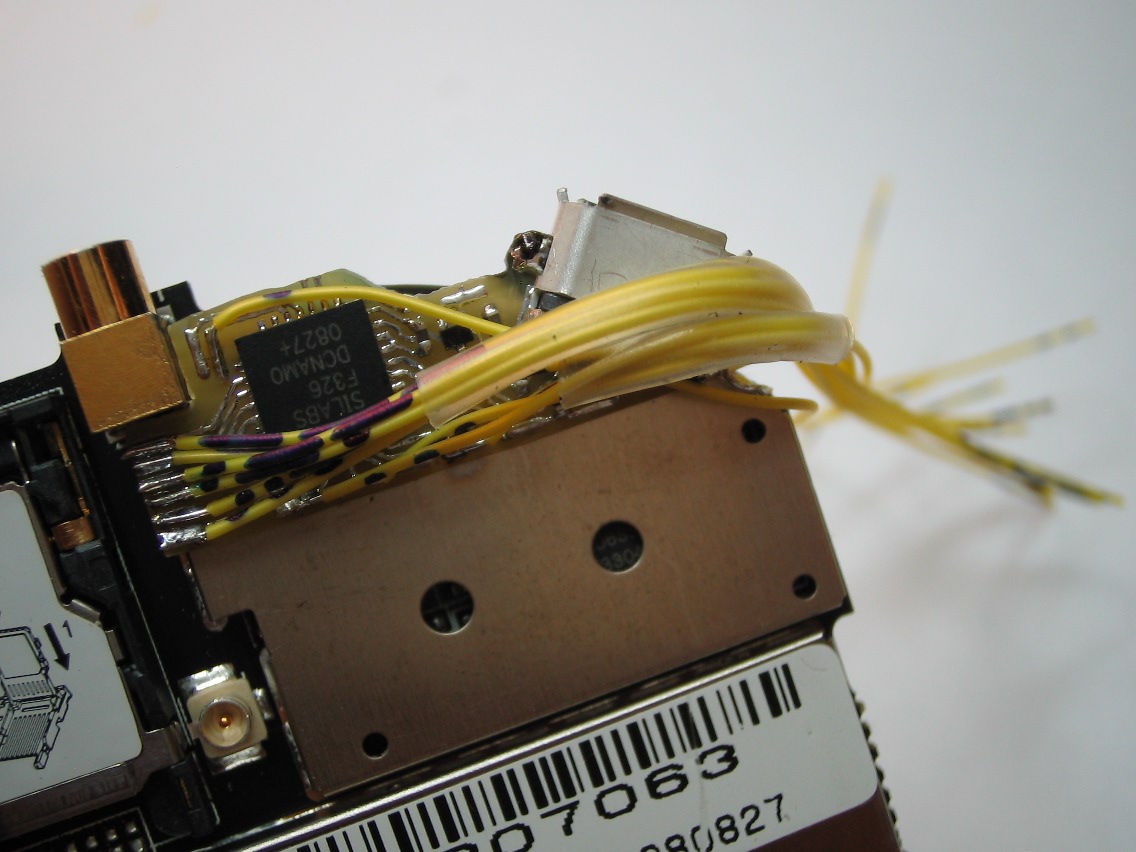
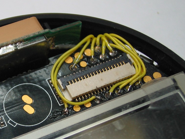
With the mechanics sorted out, we now return to the electronics.
A ground connection is added (this is the wire sticking out on the left
in the middle image below &emdash; here
is a better view of the ground connection) and thin wires are soldered
to all the pads used in this configuration. Marking both ends of each
wire with a "Morse code" as shown in the wiring diagram makes it easier
to make the right connections.


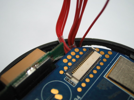
The wires are then bundled with heat-shrink tubing and brought across
the board edge to the top. (These pictures are from an earlier prototype,
hence the different color of the PCB and the much larger side hole, which
was made for Mini USB.)
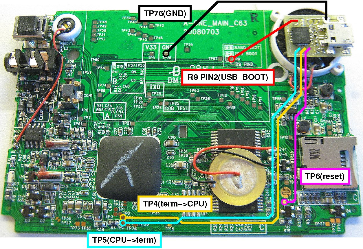
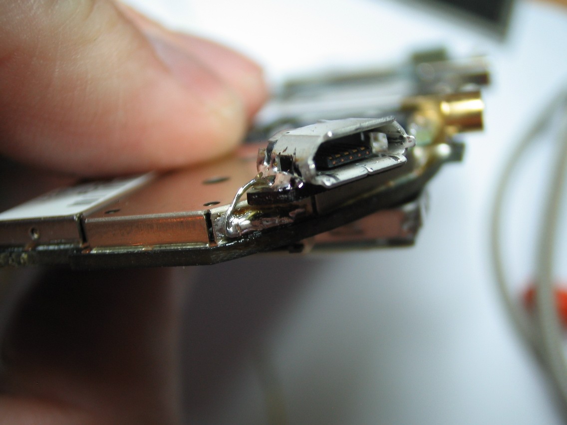
What follows is one of the highlight of the entire
operation, soldering the wires coming from IDBG to the test points on the
main PCB.
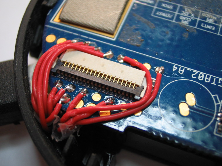
If we keep the path to the FPC connector clear, it's even
possible to have the internal debug board coexist with an external
one.
The wires shown above are stranded 30 AWG wires with an outer diameter
of 32mil or 0.8mm. This is about the thickest type of wire that can be
used &emdash; anything thicker would overflow the free space
under and around the board, and also the contacts on IDBG would be spaced
too closely. The images below show an alternative solution: wire-wrap
wires with a solid core that have an outer diameter of only about 20mil
or 0.5mm.

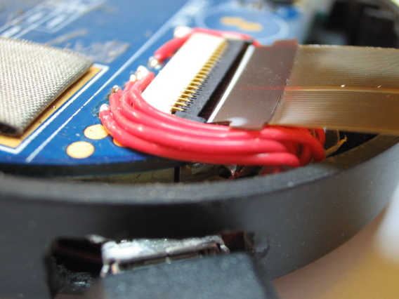
The main disadvantage of wire-wrap wires is their rigidity and thus a
higher risk of mechanical failure. The image in the middle also highlights
another problem: the isolation becomes very soft and vulnerable when heated.
If the wire is held down with a fingernail during soldering, the fingernail
may penetrate and damage the isolation. It's better to hold the wire with
something softer, e.g., the fingertip.
The last step is to close the case. There are some structures inside
the top cover that conflict with the new cables and must therefore
be removed. Their remnants have been marked with a yellow sheen in
the picture below:
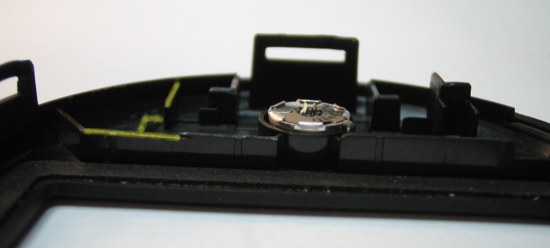
The right-hand side contains almost exactly the same structures,
which are left untouched. Note that it is not necessary to trim the
plastic wall next to the LCM if the wires are thin enough.
Gee, it still runs !

Ben NanoNote
The version for the Ben is a bit simpler and has no JTAG or I2C.
A Ben-specific addition is the connection to the USB BOOT signal.
This is what is looks like when installed:
![]()
Status
What works:
- Initial programming of the microcontroller's Flash
- Boundary scan through the
C2
interface
- Serial debugging output from the microcontroller
- USB enumeration in low-speed and full-speed mode
- IDBG firmware upload/download through DFU (with
dfu-util)
- Starting the IDBG firmware from the boot loader
- Read/write access to I/O pins through USB using the IDBG EP0 protocol
- Serial console at 115200bps
- JTAG with OpenOCD
- Read/write access to I2C devices through USB using the IDBG EP0 protocol
- Control of nNOR_WP in GTA02 through command-line utility
- If unpowered, IDBG leaks only about 10 nA through GPIOs
- f386 -p protects the boot loader from being clobbered by the firmware
What's untested or not yet done:
- Operation with IDBG connected to VSYS, especially power consumption
- GTA01 UART sharing with nGSM_EN
- Monitoring of nRESET for automatic JTAG detach
- Testing on GTA01
- Effect on GPS performance
- Find out what descriptors to use for serial console
Known bugs:
- DFU upload causes stray stalls if sending EP0-sized packets
- f326 sometimes locks up (work-around: just try again)
- Organization of code and repository isn't nice
- Need more fine-grained licensing, e.g., CC for schematics,
LGPL for libraries
- Flow control of serial console is broken in the host to target direction
For further study:
- IDBG should be able to command the PMU during power-up,
e.g., allowing it to limit inrush current and to override PMU
settings.
The idea is as follows:
- connect IDBG VSYS to the PMU's SYS1/SYS2
- remove SYS1/SYS2 from VB_SYS
- connect SYS1/SYS2 to VB_SYS through a switch, e.g., a
Fairchild FPF1003A or similar.
- control the switch via IDBG FUTURE
Since VB_SYS is hard to interrupt on GTA02, the idea could be tried by
switching only IO_3V3.
- Could we merge USB power from IDBG into VBUS ?
Some considerations:
- The PMU does not support "merging" USB and adapter power.
If adapter power is present, it takes precedence over USB.
- If we merge directly into VB_SYS and main USB is not connected,
the PMU will not charge the battery.
- If we merge into VBUS, we can share the PMU's USB current limiter.
However, if the limiter was set to the sum of the inputs, we would
overload the remaining input if the other one is disconnected.
To prevent this, we would either have to draw power from only one
USB source at a time or have external current limiters on both.
- If GTA02 provides USB power, this power is taken from VB, so
there is a conflict with accepting power from another party. We
could probably connect U4904 to VB_SYS.
- If we merge into USB_VBUS, we could feed the USB output
directly but would lose the reverse current protection of U4905.
- Could IDBG snoop the I2C bus and report transactions ?
- Consider adding special serial console functions. Some ideas:
~r to reset (GPIO), ~p to power down (PMU),
~d to dump the log buffer from a crashed kernel (JTAG), ...
Werner Almesberger,
05-MAY-2014